ETHZ/FlipFlop
From 2007.igem.org
(→An Engineer's View on Biological Learning) |
(→An Engineer's View on Biological Learning) |
||
| Line 89: | Line 89: | ||
An equivalent system behavior can be realized using [http://en.wikipedia.org/wiki/Flip-flop_%28electronics%29 flip-flops], implemented by [http://en.wikipedia.org/wiki/Logic_gate logical gates]: | An equivalent system behavior can be realized using [http://en.wikipedia.org/wiki/Flip-flop_%28electronics%29 flip-flops], implemented by [http://en.wikipedia.org/wiki/Logic_gate logical gates]: | ||
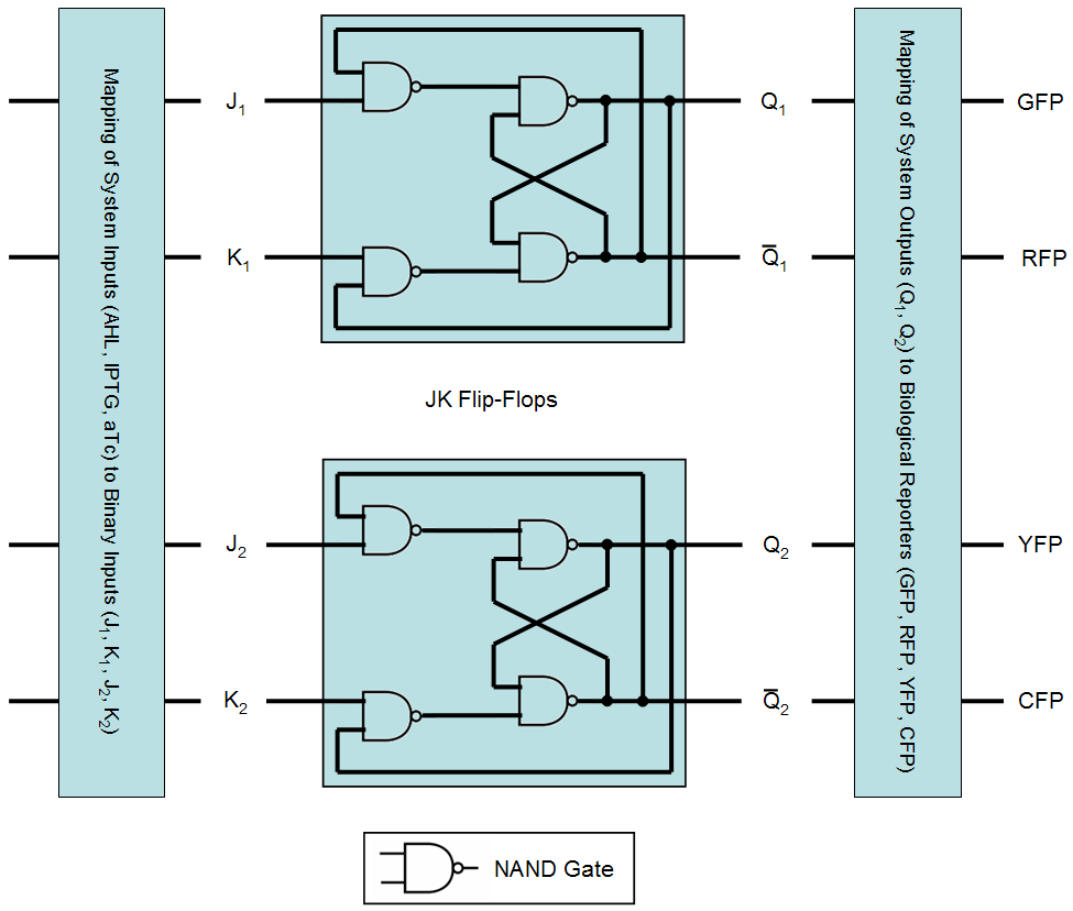
| - | As already shown in the [ | + | As already shown in the [[ETHZ/FSM | finite state machine representation]] (FSM), the proposed system consists of three different states and recognizes four different inputs. In total, this adds up to twelve different transitions. In order to implement these twelve transitions with a digital system, at least four binary inputs are required (allowing for a maximum of 16 transitions) and since the proposed system has four different outputs, at least two binary outputs are required. Here, we chose an implementation using two JK flip-flops consisting of [http://en.wikipedia.org/wiki/Nand_gate#NAND_gate NAND gates]. An overview of the resulting system is given in Fig. 1 and details concerning flip-flop and NAND gate behavior are given in the following table: |
{| class="wikitable" border="1" cellspacing="0" cellpadding="2" style="text-align:left; margin: 1em 1em 1em 0; background: #f9f9f9; border: 1px #aaa solid; border-collapse: collapse;" | {| class="wikitable" border="1" cellspacing="0" cellpadding="2" style="text-align:left; margin: 1em 1em 1em 0; background: #f9f9f9; border: 1px #aaa solid; border-collapse: collapse;" | ||
| Line 103: | Line 103: | ||
|} | |} | ||
| - | When initializing the system we set both outputs ''Q'' to zero. The mapping from inputs ([ | + | When initializing the system we set both outputs ''Q'' to zero. The mapping from inputs ([[ETHZ/FSM | AHL+IPTG, IPTG, AHL+aTc, aTc]]) and system states ([[ETHZ/FSM | ''q''<sub>0</sub>, ''q''<sub>1</sub>, ''q''<sub>2</sub>]]) to the binary inputs (J<sub>1</sub>, K<sub>1</sub>, J<sub>2</sub>, K<sub>2</sub>) is given by following table: |
{| class="wikitable" border="1" cellspacing="0" cellpadding="2" style="text-align:left; margin: 1em 1em 1em 0; background: #f9f9f9; border: 1px #aaa solid; border-collapse: collapse;" | {| class="wikitable" border="1" cellspacing="0" cellpadding="2" style="text-align:left; margin: 1em 1em 1em 0; background: #f9f9f9; border: 1px #aaa solid; border-collapse: collapse;" | ||
| Line 127: | Line 127: | ||
|} | |} | ||
| - | Here, we assume that the FSM system states ''q''<sub>0</sub>, ''q''<sub>1</sub>, ''q''<sub>2</sub> are mapped to the outputs ''Q''<sub>1</sub> and ''Q''<sub>2</sub> as follows: | + | Here, we assume that the [[ETHZ/FSM | FSM system states]] ''q''<sub>0</sub>, ''q''<sub>1</sub>, ''q''<sub>2</sub> are mapped to the outputs ''Q''<sub>1</sub> and ''Q''<sub>2</sub> as follows: |
{| class="wikitable" border="1" cellspacing="0" cellpadding="2" style="text-align:left; margin: 1em 1em 1em 0; background: #f9f9f9; border: 1px #aaa solid; border-collapse: collapse;" | {| class="wikitable" border="1" cellspacing="0" cellpadding="2" style="text-align:left; margin: 1em 1em 1em 0; background: #f9f9f9; border: 1px #aaa solid; border-collapse: collapse;" | ||
Revision as of 14:03, 26 October 2007
An Engineer's View on Biological Learning
An equivalent system behavior can be realized using flip-flops, implemented by logical gates:
As already shown in the finite state machine representation (FSM), the proposed system consists of three different states and recognizes four different inputs. In total, this adds up to twelve different transitions. In order to implement these twelve transitions with a digital system, at least four binary inputs are required (allowing for a maximum of 16 transitions) and since the proposed system has four different outputs, at least two binary outputs are required. Here, we chose an implementation using two JK flip-flops consisting of NAND gates. An overview of the resulting system is given in Fig. 1 and details concerning flip-flop and NAND gate behavior are given in the following table:
| J | K | Qnext | A | B | A NAND B | |
|---|---|---|---|---|---|---|
| 0 | 0 | Qprev | 0 | 0 | 1 | |
| 0 | 1 | 0 | 0 | 1 | 1 | |
| 1 | 0 | 1 | 1 | 0 | 1 | |
| 1 | 1 | ¬Qprev | 1 | 1 | 0 |
When initializing the system we set both outputs Q to zero. The mapping from inputs ( AHL+IPTG, IPTG, AHL+aTc, aTc) and system states ( q0, q1, q2) to the binary inputs (J1, K1, J2, K2) is given by following table:
| states/inputs | AHL+IPTG | IPTG | AHL+aTc | aTc |
|---|---|---|---|---|
| q0 | J1=0, K1=1, J2=1, K2=0 | J1=0, K1=0, J2=0, K2=1 | J1=1, K1=0, J2=0, K2=1 | J1=0, K1=1, J2=0, K2=1 |
| q1 | J1=0, K1=1, J2=1, K2=0 | J1=0, K1=0, J2=0, K2=1 | J1=0, K1=1, J2=0, K2=0 | J1=0, K1=0, J2=1, K2=1 |
| q2 | J1=1, K1=0, J2=0, K2=0 | J1=1, K1=1, J2=0, K2=0 | J1=1, K1=0, J2=0, K2=1 | J1=0, K1=1, J2=0, K2=1 |
Here, we assume that the FSM system states q0, q1, q2 are mapped to the outputs Q1 and Q2 as follows:
| FSM states/output coding | Q1 | Q2 |
|---|---|---|
| q0 | 0 | 0 |
| q0 | 0 | 1 |
| q0 | 1 | 0 |
The final mapping from transitions to the biological reporters is then given by:
| J1=0, K1=1, J2=1, K2=0 | J1=0, K1=0, J2=0, K2=1 | J1=1, K1=0, J2=0, K2=1 | J1=0, K1=1, J2=0, K2=1 | J1=0, K1=1, J2=1, K2=0 | J1=0, K1=0, J2=0, K2=1 | J1=0, K1=1, J2=0, K2=0 | J1=0, K1=0, J2=1, K2=1 | J1=1, K1=0, J2=0, K2=0 | J1=1, K1=1, J2=0, K2=0 | J1=1, K1=0, J2=0, K2=1 | J1=0, K1=1, J2=0, K2=1 |
|---|---|---|---|---|---|---|---|---|---|---|---|
| cyan | cyan | red | cyan | cyan | cyan | yellow | green | cyan | cyan | cyan | yellow |

